


CA-IS3211SCG

Active
Single-channel, Opto-compatible Isolated Gate Driver
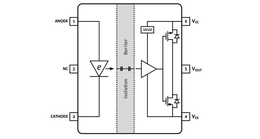
The CA-IS3211 devices are a family of single-channel, optocompatible isolated gate driver capable of sinking 6A andsourcing 5A currents. These devices operate with dualsupplies or a single supply of 10V to 30V (8V UVLO version)or 14V to 30V (12V UVLO) wide voltage range of VCC - VEE,making them ideal to drive power MOSFET, IGBT or siliconcarbide(SiC) transistors in various inverter, motor control orisolated power supply systems. The CA-IS3211 can beconfigured as low-side and high-side drivers. The CAIS3211V_ offers single terminal gate drive output: VOUT andthe CA-IS3211S_ offers dual separate output terminals:OUTH and OUTL. The driver output is pulled to low state toturn-off external power transistors when VCC supply input iseither not powered, is open-circuit or is in UVLO.
All devices have integrated digital galvanic isolation usingChipanalog’s proprietary capacitive isolation technologyand feature isolation for a withstand voltage rating of up to5.7kVRMS for 60 seconds with minimum common-modetransient immunity (CMTI) of 150kV/μs. These devices canbe used as drop-in replacement for the industry standardoptocoupler-based gate drivers while providing high CMTI,low propagation delay, small pulse width distortion andsmall part-to-part skew. The input stage is an analog diodewhich means long term reliability and excellent agingcharacteristics.
The CA-IS3211 devices are available either in a 6-pin or 8-pin wide-body SOIC packages, and 8-pin DUB package. Alldevices are rated for operation at junction temperatures of-40°C to +150°C.


-
Features
6A Peak Sink Current and 5A Peak Source Current
Up to 30V Output Drive Supply Range with 8V (CAIS3211VB_) and 12V (CA-IS3211VC_) UVLO options
Support Rail to Rail Output
Up to 7V Reverse Voltage on Input-stage
Matching Propagation Delay
70ns Propagation delay (typical)
25ns Part to part propagation delay matching (maximum)
35ns Pulse width distortion(maximum)-40°C to +150°C Operating Junction Temperature Range
Robust Galvanic Isolation
High lifetime: >40 years
Up to 5.7kVRMS isolation rating for the wide-body packages and up to 3.75 kVRMS isolation rating for CA-IS3211VCU
Common-mode transient immunity (CMTI) >±150kV/μsPackage options
6-pin wide-body SOIC (J) Package
8-pin wide-body SOIC8 (G) Package
8-pin SOP (DUB) packageSafety regulatory approvals
8000 VPK reinforced isolation per DIN V VDE V0884-17: 2021-10 (wide-body SOIC)
5300 VPK basic isolation per DIN V VDE V0884-17:2021-10 (DUB8)
5.7 kVRMS isolation for 1 minute according to UL1577 (wide-body SOIC)
3.75 kVRMS isolation for 1 minute according to UL 1577(DUB8)
TUV certification per EN61010-1:2010+A1 -
Applications
-
Isolated DC-DC and AC-DC Converters
-
Motor Contro
-
Uninterruptible Power Supply (UPS)
-
Isolated Gate Driver for Inverters
-
-
Device Information
Part Number Package Package Size(NOM) CA-IS3211VBJ SOIC6-WB 7.5 mm x 4.68 mm CA-IS3211VCJ SOIC6-WB 7.5 mm x 4.68 mm CA-IS3211VBG SOIC8-WB 7.5 mm x 5.85 mm CA-IS3211VCG SOIC8-WB 7.5 mm x 5.85 mm CA-IS3211SBG SOIC8-WB 7.5 mm x 5.85 mm CA-IS3211SCG SOIC8-WB 7.5 mm x 5.85 mm CA-IS3211VBU DUB8 6.35 mm x 9.2 mm CA-IS3211VCU DUB8 6.35 mm x 9.2 mm -
Simplified Functional Diagram
-
Technical Documentation
Category
Title
Last Updated
-
Title: APPNOTE
Last Updated: Jul 23,2024
-
Title: Datasheet
Last Updated: Nov 21,2023
-
-
Certification Standards
Category
Title
Certification Number
Date
-
Title: TÜV-EN IEC 62368
Certification Number: AK 50656801 0001
Date: Dec 26,2024
-
Title: CQC
Certification Number: CQC24001434134
Date: Jun 06,2024
-
Title: VDE
Certification Number: 40057278
Date: Aug 21,2023
-
Title: UL
Certification Number: UL-US-L511334-11-71100202-9
Date: Sep 06,2023
-