 Interface
  Isolated Interface
  Digital Isolation
  Isolated Sensing
  Signal Chain
  Sensor
  Isolated Driver
  Power Management
  Driver & Switch



CA-IS3211CVBJ
CA-IS3211CVBJ

Active
4.7A Source /6A Sink, 5.7kVRMS Opto-Compatible Single-Channel Isolated Gate Driver
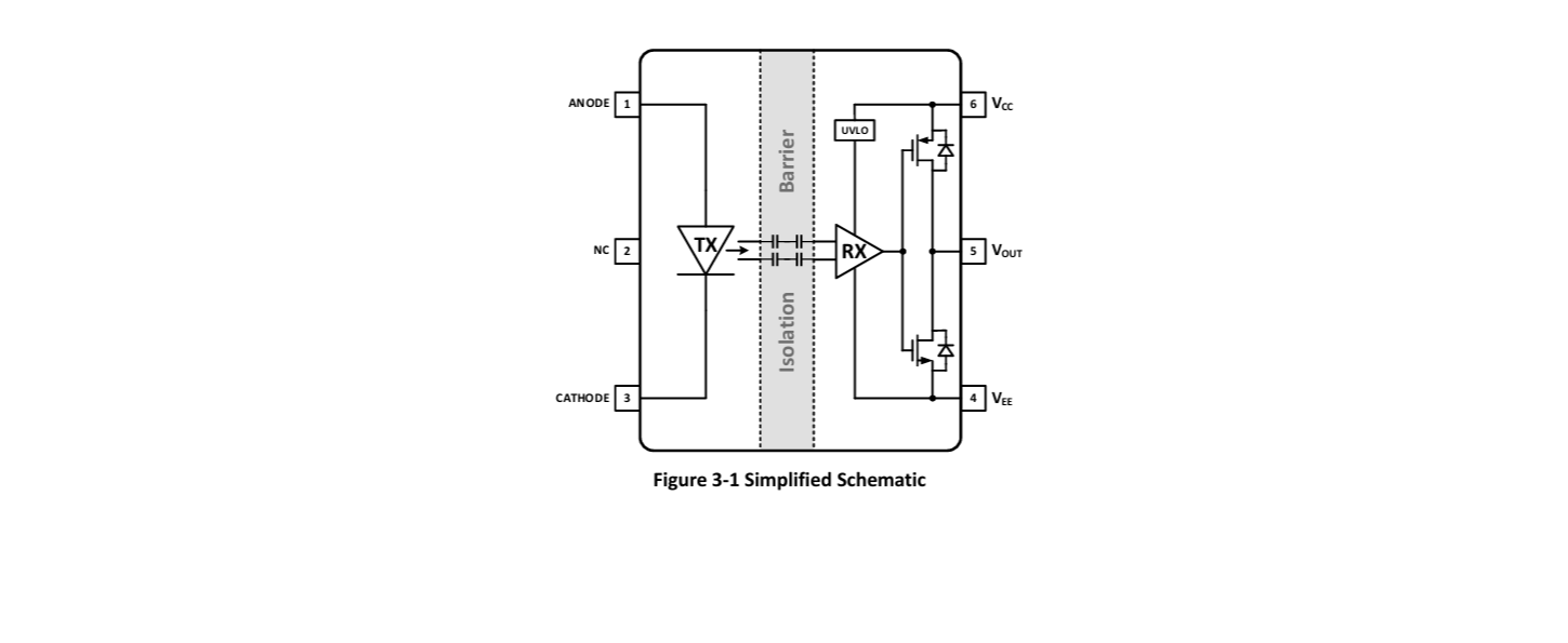
The CA-IS3211C devices are a family of single-channel, opto- compatible isolated gate driver capable of sourcing 4.7A and sinking 6A currents. These devices operate with dual supplies or a single supply of 10V to 30V (8V UVLO version) or 14V to 30V (12V UVLO version) wide voltage range of VCC - VEE, making them ideal to drive power MOSFET, IGBT or silicon-carbide (SiC) transistors in various inverter, motor control or isolated power supply systems. The CA-IS3211C can be configured as low-side and high-side drivers. The CA IS3211CVx offers single terminal gate drive output: VOUT and the CA-IS3211CSx offers dual separate output terminals: OUTH and OUTL. The driver output is pulled to low state to turn-off external power transistors when VCC supply input is either not powered, open-circuit or in UVLO.
The CA-IS3211C devices have integrated digital galvanic isolation using Chipanalog’s proprietary capacitive isolation technology and feature isolation with a withstand voltage rating of up to 5.7kVRMS/3.75kVRMS for 60 seconds and minimum common-mode transient immunity (CMTI) of 150kV/μs. These devices can be used as drop-in replacement for the industry standard optocoupler-based gate drivers while providing high CMTI, low propagation delay, small pulse width distortion and small part-to-part skew. The input stage is an analog diode which means long term reliability and excellent aging characteristics.
The CA-IS3211C devices are available either in a 6-pin or 8 pin wide-body SOIC packages, and 8-pin DUB package. All devices are rated for operation at junction temperatures of -40°C to +150°C.



-
Features
4.7A Peak Source Current and 6A Peak Sink Current
Up to 30V Output Drive Supply Range with 8V and 12V UVLO options
Support Rail to Rail Output
Up to 7V Reverse Voltage on Input-stage, Interlock
Matching Propagation Delay
80ns Propagation delay (typical)
25ns Part to part propagation delay matching (maximum)
35ns Pulse width distortion (maximum)-40°C to +150°C Operating Junction Temperature Range
Robust Galvanic Isolation
High lifetime: >40 years
Up to 5.7kVRMS isolation rating for the wide-body packages and 3.75kVRMS isolation rating for DUB8 package
Common-mode transient immunity (CMTI) > ±150kV/μsPackage options
6-pin wide-body SOIC6-WB (J) package
6-pin wide-body TSOIC6-WB (TJ) thin package
8-pin wide-body SOIC8-WB (G) package
8-pin DUB8 (U) package -
Applications
-
Isolated DC-DC and AC-DC Converters
-
Motor Control
-
Uninterruptible Power Supply (UPS)
-
Isolated Gate Driver for Inverters
-
-
Device Information
Part Number Package Package Size (NOM) CA-IS3211CVBJ SOIC6-WB (J) 4.68mm x 7.50mm x 3.18mm CA-IS3211CVCJ SOIC6-WB (J) 4.68mm x 7.50mm x 3.18mm CA-IS3211CVBTJ TSOIC6-WB (TJ) 4.68mm x 7.50mm x 2.30mm CA-IS3211CVCTJ TSOIC6-WB (TJ) 4.68mm x 7.50mm x 2.30mm CA-IS3211CVBG SOIC8-WB (G) 5.85mm x 7.50mm CA-IS3211CVCG SOIC8-WB (G) 5.85mm x 7.50mm CA-IS3211CSBG SOIC8-WB (G) 5.85mm x 7.50mm CA-IS3211CSCG SOIC8-WB (G) 5.85mm x 7.50mm CA-IS3211CVBU DUB8 (U) 9.20mm x 6.62mm CA-IS3211CVCU DUB8 (U) 9.20mm x 6.62mm -
Simplified Functional Diagram