 Interface
  Isolated Interface
  Digital Isolation
  Isolated Sensing
  Signal Chain
  Sensor
  Isolated Driver
  Power Management
  Driver & Switch


CA-IF1169FDT-Q1
CA-IF1169FDT-Q1

Active
High-speed CAN System Basis Chip with LDO and Watchdog
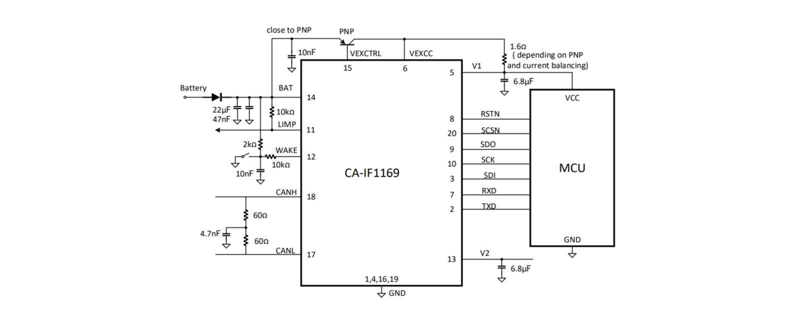
The CA-IF1169 is a system basis chip(SBC) with integrated high-speed CAN(controller area network) transceiver and dual LDOs. The CAN transceiver complies with ISO 11898- 2:2016 and SAE J2284-1 to SAE J2284-5 standards for high-speed CAN physical layer specifications, supporting up to 5 Mbit/s CAN FD communication. These devices feature up to ±42V extended fault protection on the data transmission lines in all operation modes. Also, the dominant timeout detection can prevent bus lockup caused by controller error or by a fault on the TXD input.
The CA-IF1169 SBC can operate in different modes: normal operation, reset mode, overtemperature protection mode, and standby/sleep modes for low current consumption. In the low-power standby and sleep modes, the CA-IF1169 supports remote wake-up (WUP) or selective wake-up frame(WUF) as defined by ISO 11898-2:2016, and local wake-up through the WAKE pin.
The CA-IF1169 integrates two low-drop voltage regulators (LDO V1 and LDO V2). LDO V1 provides 3.3V or 5V output voltage option with up to 250mA output current capability, see Table 5-1. Ordering Information. Also, its current capacity can be extended via an external PNP transistor, enabling it to power the system microcontroller or other on-board loads. LDO V2 provides 5V output voltage with up to 100mA output current to support the internal CAN transceiver and other loads supply. Internal LDO output option simplifies the interface with 3.3V or 5.0V CAN controllers. SPI-compatible interface is available for transceiver operation control and status information reading.
The CA-IF1169 follows a comprehensive functional safety development process with integrated analog circuit initiate self-test (ABIST), critical interface monitoring. The dedicated LIMP output pin for failure indication can be used to guide the system into limp-home mode. These devices comply with ISO 26262 ASIL-B standard and support customer to achieve ASIL-B certification for their end products.
The CA-IF1169 family of devices is available in 20-pin DFN package, operates over the -55°C to +150°C junction temperature range.


-
Features
Meets the requirements of ISO 11898-2:2016 and SAE J2284-1 to SAE J2284-5 physical layer standards
ASIL-B compliant: designed with complete functional safety development process, supporting customer to achieve ASIL-B certification
CAN FD Support
enables CAN FD data transmission up to 5 Mbit/s
Support selective wake to wake-up specific partial networking nodes
CAN bus pins short-circuit protection to ±42 V, ideal for 12V battery systems
Autonomous bus biasing
Integrated dual low-drop voltage regulators (LDO)
LDO 1 (V1): 3.3V and 5V output voltage option with up to 250mA output current capability. Supports current extension via an external PNP transistor for increased output capacity, to provide power supply for system microcontroller or other loads
LDO 2 (V2): 5V output voltage with up to 100mA output current capability, provide power supply for internal CAN transceiver and other loads.Advanced ECU power management
Ultra-low power consumption in sleep mode: 12.8µA (typical)
Remote wake-up via standard CAN wake-up pattern(WUP) or selective wake-up frame (WUF) according to ISO 11898-2:2016
Selective wake supports 50kbit/s, 100kbit/s, 125kbit/s, 250kbit/s, 500kbit/s and 1Mbit/s CAN bit-rate
Local wake-up via WAKE terminal, also local wake-up can be disabled to reduce power consumption
Wake-up sources identificationIntegrated protection and diagnosis increase system robustness
16/24/32 bit SPI-compatible interface for device configuration, control and events diagnosis
Transmitter dominant timeout prevents lockup
Configurable watchdog timer
Cyclic wake-up in watchdog timeout mode
Overtemperature shutdown and alarm
Undervoltage protection on BAT supply terminal
LDO V1/LDO V2 overvoltage and undervoltage detection and protection
Cold start-up detection (PO and NMS bits)
Battery, WAKE and CAN bus pins protected against transients according to ISO 7637-3, test pulses 1, 2a, 3a and 3b
Advanced system and transceiver interrupt process
Integrated analog circuit initiate self-test (ABIST) and stuck monitoring on critical interfaces.Dedicated LIMP output to indicate system failure and guide the system into limp-home mode
Multiple time programmable(MTP) non-Volatile(NV) memory
Support multiple online debugging configuration and two-times programmability
Configurable power-up and reset behaviors and the system basis chip operating modes for different applications–40°C to 150°C junction temperature range
Complies with the AEC-Q100 Grade 1 standard for automotive applications
Available in DFN20 package (wettable flank)
-
Applications
-
Body electronics
-
Automotive lighting systems
-
Advanced driver assistance systems (ADAS)
-
Thermal management systems for new energy vehicles
-
Automotive sensors
-
In-car entertainment systems
-
Automotive power train systems
-
-
Simplified Functional Diagram
-
Certification Standards
Category
Title
Certification Number
Date
-
Title: Reliability Test
Certification Number: CA-IF1169X-Q1_V1.0
Date: Apr 14,2026
-