


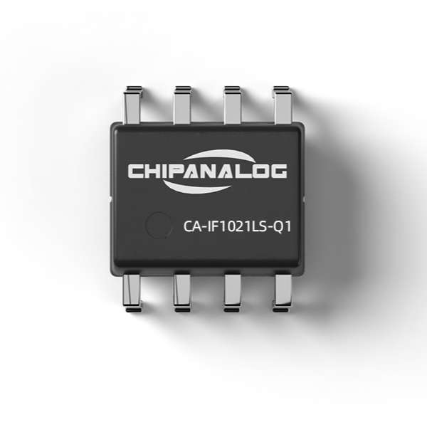
CA-IF1021LS-Q1
CA-IF1021LS-Q1

Preview
LIN Transceiver
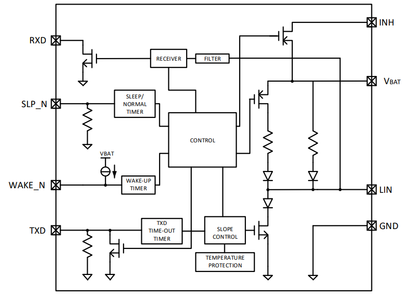
The CA-IF1021Lx-Q1 family of device is Local Interconnect Network (LIN) transceiver with integrated wake-up and protection features for automotive applications. LIN is low-speed universal asynchronous receiver transmitter (UART) communication protocol used to support in-vehicle networks. The CA-IF1021Lx-Q1 transceiver controls the LIN bus state via the TXD input and reports the bus state on its open-drain output RXD between the protocol controller and physical LIN networks. These device features slew-rate control and wave-shaping to reach a very low level of electromagnetic emission (EME) within a broad frequency range.
The CA-IS1021x-Q1 devices are designed to support 12V automotive applications with 5.5V to 27V wide VBAT input voltage operating range and have up to ±42V fault protection on LIN bus, with integrated ESD protection, these devices help to reduce external components in the design. Also, these devices feature low-power sleep mode, as well as wake-up capability over LIN bus, or via the WAKE_N pin, SLP_N pin. Inhibit output (INH) can be used to control one or more external voltage regulators presented on a node to reduce the battery power consumption at system level. In the event of a ground shift or supply voltage disconnection, the devices can prevent back-feed current through LIN to the supply input.
The CA-IF1021Lx-Q1 transceiver is available in a standard 8- pin SOIC package and 8-pin DFN package, operates over the -40°C to +150°C junction temperature range.


-
Features
Meets LIN2.0、LIN2.1、LIN2.2、LIN2.2A and ISO 17987-4:2016(12V) Physical-layer (EPL) Standards
Compliant to SAE J2602-1 and SAE J2602-2 LIN Physical-layer Specification
Designed to Support 12V Applications with Wide Operating Supply Range
5.5V to 27V supply range (VBAT)
3.3V and 5.0V Input Logic Compatible
System-level Power Control via INH pin
Power-up/down Glitch-free Operation on LIN bus and RXD output
Integrated 30kΩ LIN pull-up Resistor
Support up to 20kbps LIN Transmission Data Rate
Operating Mode
Normal operation
Low-power sleep
Low-power standby
Power-onWake-up from Low-power Mode
Remote wake-up via LIN bus
Local wake-up via WAKE_N or SLP_N pinsIntegrated Protection Increases Robustness
±42V fault-tolerant LIN bus
42V load dump protection
Enhanced ESD protection
Undervoltage protection on VBAT
Transmitter dominant timeout prevents lockup
Thermal shutdown
System level fail-safe protection for the unpowered node or ground disconnection–40°C to 150°C Junction Temperatures Range
Available in SOIC8 and DFN8 (3.0mm x 3.0mm) Packages
-
Applications
-
Body electronics
-
Automotive gateway
-
Infotainment and cluster
-
Hybrid electric vehicles and powertrain systems
-
-
Device Information
Part number
Package
Package size(NOM)
CA-IF1021LS-Q1
SOIC8(S)
4.9mm x3.9mm
CA-IF1021LD-Q1 DFN8
3mm*3mm
-
Simplified Functional Diagram
-
Technical Documentation
Category
Title
Last Updated
-
Title: Datasheet
Last Updated: Jul 10,2024
-
-
Certification Standards
Category
Title
Certification Number
Date
-
Title: Reliability Test
Certification Number:
Date: Jan 10,2025
-